Introduction
How you do this is up to you, however if you're like me and using advanced devices that come only in surface mount form then a PCB is the only way to go!
Designing a custom PCB is simple. However getting it made can be complicated. If you're lucky you know someone at university who can slide your project under the table when no one is watching. If you're less lucky you have to pay someone to make it and prices for one-off boards can be prohibitive.
But if you have access to a laser printer, some glossy photo paper and a domestic iron then you're in luck! Just follow my step by step guide!
Recommendations for making artwork
Oddly enough, the finer your board, the more likely it is to succeed!
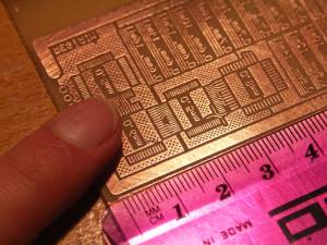
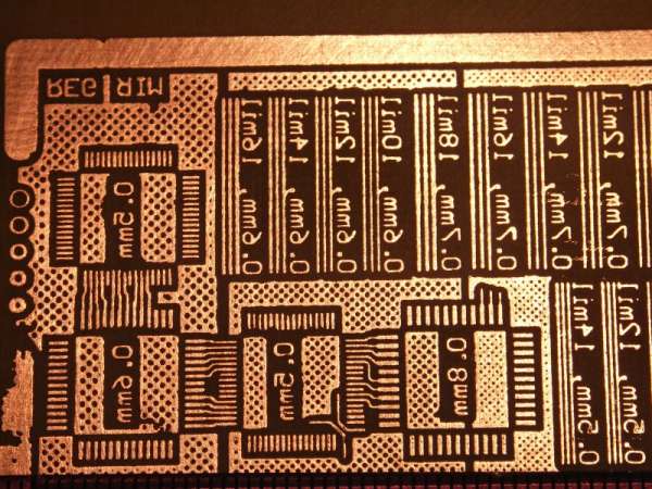
Highly recommended is a polygon plane (aka a ground plane), created with 45° cross hatching, 12-15mil lines at 25-30mil spacing. Don't turn on the option to remove "dead copper". Net-to-net spacing should be 12-20mil, although I have successfully etched boards with 0.5mm track pitch.
Any text should be mirrored (if on the bottom layer) but the final pattern should be printed without mirroring or negative options enabled.
The choice of paper is important; I'm using Kodak "Picture Paper" which at 190gsm is horrible! What is important is that the paper is shiny and smells funny. This allows us later on to remove the paper while leaving the toner attached to the board.
Why is a finer pattern better?
I've found that when transferring the toner to a PCB, areas without any toner don't stick to the paper. Once the iron is removed the expanding gases and different expansion/contraction rates of the paper & board cause areas without toner to buckle and produce bubbles. The upwards pressure of these bubbles on the surrounding toner can act to lift surrounding tracks, causing annoying voids on the completed board!
By making the space between tracks very fine and using a ground plane, this can easily be avoided.
Another point is to use a cross hatched ground plane rather than a solid one, as the individual tracks in the cross hatching appear to grip better than one solid area of toner. They also seem to print better on older priters. I've found that if for any reason part of a solid ground plane should fail to stick to the copper and is lifted with the paper when removed, it will tend to take surrounding areas of the toner with it as well. By using a cross hatched ground plane I suspect this would be less likely.
Step by step guide
Part way through removing the paper.
- Design your PCB artwork (following recommendations above) and print onto glossy inkject photo paper on a laser printer. Do not flip, rotate or reverse the output.
- Clean your PCB with steel wool and meths or similar to remove all finger grease etc. Do not touch board with fingers once done.
- Iron artwork onto PCB with a very hot iron, slowly, going over every square inch with the tip of the iron applying lots of pressure, till you can see the shape of the track through the top of the photo paper.
- Do that for 10 mins or so.
- Then remove the iron and clamp the life out of it (heh... till the clamps break!) till it cools. Give it about 30 mins.
- Remove the board and place in water (cold with a little dish wash detergent if wanted).
- Leave in water for half an hour while you make dinner... peel off the top layer of paper, leaving approximately half the thickness still on it.
- Leave that to soak for another half hour or so.
- Then gently rub off the remaining paper with your fingers. Start off gentle and use more force as needed.
- For getting the bits of paper out between TQFP (as fine as 0.5mm pin pitch!) use a scrubbing brush in a rotary fashion in the direction of the tracks, "clicking" the paper out.
- Then etch! Read directions on pack. I used Ferric Chloride. Stains good. Dangerous to health. Etc.
- Etching takes about 10-12 mins with good hot-ish solution. Gently rock the solution over the board to get even faster results. Check every minute during the last few minutes of the process. You want your large sections to get etched but don't want to lose finely detailed tracks either.
- Once etched wash clean with lots of water, then remove the toner still on the board with steel wool. Give another quick wash then you're ready to drill and tin the board! Well done!
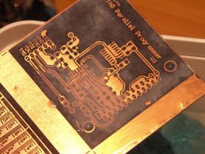
An example of what is possible — the finest tracks here are 0.25mm wide with even less space between them!
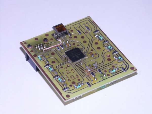
Completed SMT board